




By TechNews Editor | Published in Innovation & Hardware
As massive AI models and hyperscale cloud workloads continue to expand, hardware engineers face a physical bottleneck that traditional electrical interconnects can no longer overcome: the thermal and bandwidth limits of copper wiring. Transmitting gigabytes of electrical data across copper traces inside server racks generates intense heat and consumes a substantial portion of overall system energy.
To bypass electrical resistance, the semiconductor industry is commercializing Silicon Photonics—integrating microscopic optical waveguides directly onto silicon chips to transmit data using light instead of electricity.
The Physical Limits of Copper Interconnects
For decades, metal wires handled all data movement between processors, memory modules, and network switches. However, as compute speeds enter the terabit era, electrical signals traveling through copper suffer from severe attenuation and signal degradation.
According to research published by Optica, traditional copper connections require heavy signal equalization and active cooling to maintain data integrity over short distances. This electrical friction creates a bandwidth wall that limits high-density AI cluster performance.
How Photonic Integrated Circuits (PICs) Work
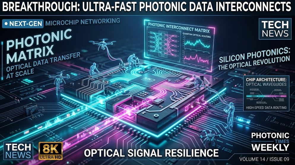
Silicon photonics merges optical communications directly with standard complementary metal-oxide-semiconductor (CMOS) manufacturing processes. As outlined on Wikipedia’s Silicon Photonics overview, Photonic Integrated Circuits (PICs) replace electrical traces with microscopic optical channels:
- On-Chip Lasers & Modulators: Converting electrical data streams into high-frequency light pulses at the silicon die level.
- Silicon Waveguides: Routing laser beams through etched silicon channels with near-zero loss and zero electromagnetic interference.
- Co-Packaged Optics (CPO): Placing optical transceivers directly alongside GPU and CPU dies on a shared substrate, reducing signal transmission distances from centimeters to millimeters.
Further technical breakdowns on optical switching architecture can be explored via the IEEE Photonics Society.
Transforming AI Cluster Infrastructure
The immediate impact of silicon photonics is most pronounced in modern enterprise AI infrastructure:
- Massive Energy Savings: Optical interconnects consume up to 70% less energy per bit transferred compared to traditional copper transceivers.
- Unprecedented Bandwidth Density: A single optical fiber channel can carry multiple light wavelengths simultaneously using Wavelength Division Multiplexing (WDM), dramatically boosting throughput.
- Ultra-Low Latency: Data traveling at the speed of light eliminates electrical signal delays across multi-rack supercomputing clusters.
As explored in our ongoing hardware breakdowns in Tech today, coupling silicon photonics with high-density NPU accelerators is key to building sustainable future data centers.
Looking Ahead: The Optical Compute Era
Silicon photonics is shifting from a specialized networking technology into a mainstream compute requirement. Major foundries are retrofitting existing silicon fabrication lines to print optical components directly onto wafer dies.
By replacing resistive copper with high-speed optical architecture, silicon photonics lays the foundation for the next decade of scaling in artificial intelligence and high-performance computing.